
28 Jun Micro Machining – Manufacturing of Mesa Diodes
Crystal Mark, Inc. has very well developed process to manufacture mesa diodes using specific masking materials.
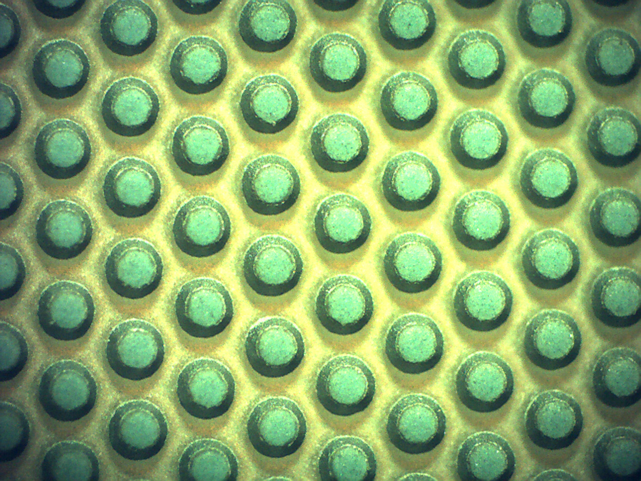
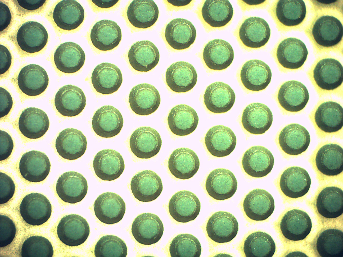
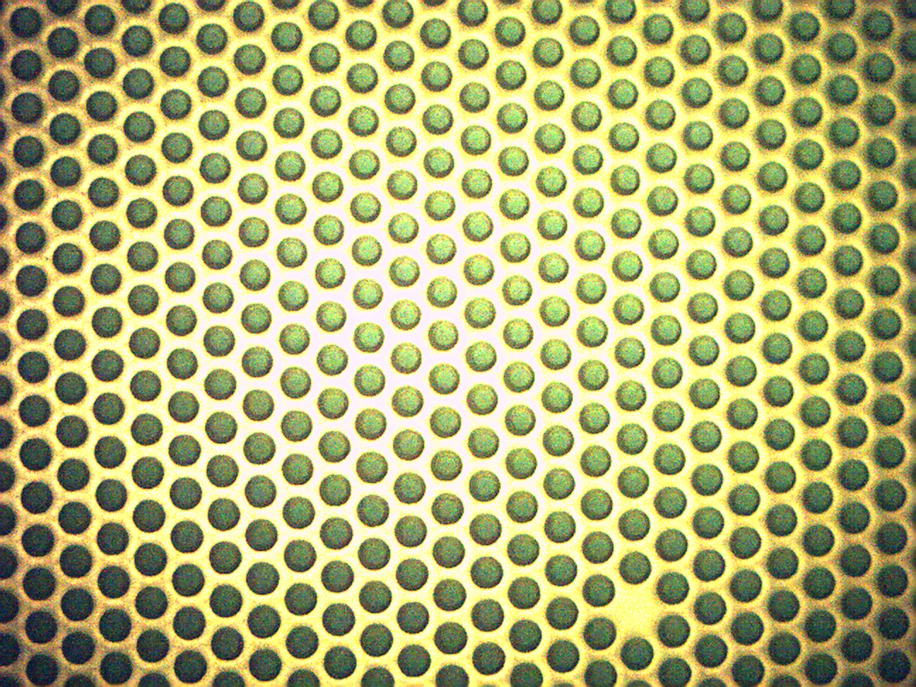
Images below show microscopic images of mesa diodes manufactured using SWAM® C1216 belt abrader. The top of the mesa in this example is 0.019” (482 microns) and the bottom is 0.027” (684 microns).
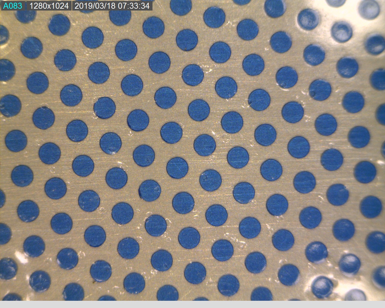
Substrate Wafer with Masking Material – Microscopic Image Taken Before the Micro Abrasive Processing
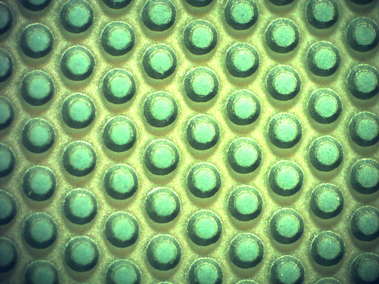
Microscopic View – After Micro Machining using Micro Abrasive Blasting Process
Micro Machining using Micro Abrasive Blasting Process
Micro Machining using Micro Abrasive Blasting Process
The technique can be used in patterning and glass, other flat parts, fluidics channels, machining different substrates, MEMS packages, control channels, patterning electrodes, piezo ceramics such as PZT (Lead Zirconate Titanate) or Barium Titanate, developing ultrasonic transducers, ceramic capacitors, etc.
For different production rates, customers also have options to use C129, C149 or C169 SWAM® Automated Systems as well.